This article talks about SEE in complex devices. It mainly focuses on Single Event Burnout (SEB) in power MOSFETs and also touches on Single Event Upset (SEU) and Single Event Functional Interrupt (SEFI) in FPGAs. SEB in power MOSFETs is always accompanied by melting of metal layers on the front side of the device when a charged particle like a proton or an uncharged particle like a neutron hits a sensitive region in the MOSFET’s channel region which causes a forward bias in the source-body junction (Reference 1). Figure 1 shows the melting of metal layers in front of the power MOSFET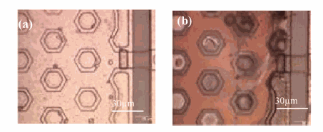 Figure 1: SEB in power MOSFETS. The right picture shows the melting of metal layers after the laser shot (Reference 1)
When the radiation testing is done to find SEB in power MOSFETS, usually the device is bombarded from the top side since the sensitive region is most likely closer to the top surface than the bottom surface of the die. The top layer is normally covered with metal layers which is not an issue for particles to pass through. However, the depth of penetration is limited and if the sensitive spot is deeper than 100 mm, it will be challenging for a moderately energetic particle to get there. Near-IR photons can penetrate through much larger depth of the die of the order of a few hundred microns, but can not penetrate through metal layers. For this reason, it is advisable to illuminate the decapsulated chip through its back side which does not have any metal coverage. Depth sensitivity measurements at a fixed voltage and varying laser pulse energy can be done to find the most sensitive depth at which the SEB occurs. Figure 2 shows the results of such measurements (Reference 1). In this measurement a 1064 nm laser of 4 mm spot size has been used. The focusing depth has been varied to find the lowest energy at which SEB occurs for a particular bias voltage
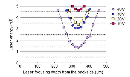
Figure 2: Depth sensitivity measurement for a power MOSFET
As seen in figure 2, different bias voltages have been used and for all of them, the lowest laser energy that triggers SEB occurs at a depth of 340 mm. The required laser energy is reduced as the Drain-Source voltage increases because SEB occurrence is easier at higher VDS voltages. This test is useful for estimating the penetration depth for the radiation testing as well. The die thickness is 430 mm, so for the radiation testing that is done through the front surface, the particle should reach a depth of 90 mm from the top. One has to make sure that the particle has enough energy to reach this depth.
Another interesting measurement is to find the minimum laser energy required to trigger SEB at a fixed power supply voltage. Figure 3 shows the result of this measurement.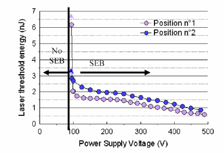
As can be seen figure 3, at a bias voltage of nearly 100 volts, regardless of what the laser pulse energy is, SEB can not be triggered. The curve shows an asymptotic behavior. As the bias voltage increases, the required laser pulse energy to trigger SEB is decreased as expected. The two curves are slightly shifted with respect to each other because they represent two different points on the chip and there is non-uniformity in the sensitivity of the structure (Reference 1).
One can also do a 2D backside laser mapping of the chip at a fixed laser energy and varying voltages as shown in figure 4 (Reference 2).
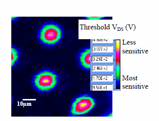
When the charges created by an ionizing track are deposited near the channel region of a POWER MOSFET, they cause forward biasing of the source-body junction and hence SEB occurs. On the other hand, when these charges are deposited in the plug region, the holes are directly collected at the body contact and do not contribute to the forward biasing of the source-body junction. This explains the sensitivity of the channel area and the insensitivity of the plug area (Reference 2).
It is also possible to compare the cross sections measured by a fixed laser energy as a function of bias voltage with the cross section of a fixed energy ion beam as a function of bias voltage (Reference 2). Figure 4 shows the results:
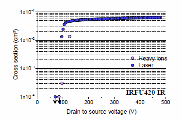
Figure 5: Comparison of cross section measured by laser method and heavy ion beam.
Both curves nearly coincide and this proves the compatibility of the two methods. For the above optical method of cross section measurement, the energy of the laser pulse was 6 nj and for the radiation method of cross section measurement, a high LET beam of sufficient range was used.
Near-IR pulsed lasers can also be used to probe the configuration memory of FPGAs for laser induced SEU and SEFI. In one study a pulsed laser of 1064 nm was shone on the configuration memory of an FPGA programmed for a particular task (Reference 3). Not only the laser pulse caused SEU in the configuration memory but it was found that 14% of the cells that experienced SEU, also caused a disruption in the task to be performed and hence caused a SEFI.
Allied Scientific Pro provides laser testing systems for probing Single Event Effect in space electronics. Both Single Photon Absorption (SPA) and Two Photon Absorption (TPA) systems are offered. The following link contains more information about the offered systems.
The SPA laser is a 1030 nm fiber laser capable of emitting pulses of pico-second duration and nano-joules energy. There is also a SPA lab which is available for rental. The lab contains a 1030 nm fiber laser, SWIR and visible cameras, precise motion controllers, high power microscope objectives and illuminators.
References:
1- Characterization of Single-Event Burnout in Power MOSFET Using Backside Laser Testing, F.Miller et.al, IEEE transactions on nuclear science, VOL.53, NO. 6, December 2006.
2- SEB characterization of commercial power MOSFETs with backside laser and heavy ions of different ranges, A. Luu et.al, IEEE transaction on nuclear science, September 2008.
3- Pulsed-Laser Testing for Single-Event Effects Investigations, Stephen Buchner et.al, IEEE transactions on nuclear science, VOL.60, NO 3, June 2013.