Understanding the Single Event Effect (SEE)
Space-born instruments carry many electronic devices including micro-processors, registers in digital circuits, etc. If a charged particle from space, strikes a sensitive node of an electronic circuit, it may cause a disruption or a permanent damage. This article intends to explain this issue. Our sun emits a large number of charged and uncharged particles including protons, heavy ions and neutrons. Aside from that there is a stream of charged particles from cosmic rays that bombard the Earth constantly. Many of these charged particles get trapped in the Earth’s magnetic field and constantly circle around the planet. The Earth’s Van Allen Belt, which traps these charged particles, is shown in figure 1
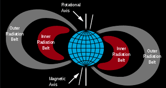
Figure 1: Earth’s Van Allen Belt (Wikipedia picture)
As depicted in the figure, the Earth’s magnetic field is slightly offset from the planet’s axis and the Van Allen belt consists of an inner belt and an outer belt. In addition, neutrons reaching the surface of the Earth could also collide with an atom and produce a destructive secondary charged particle [Reference 1]. If necessary precaution in the from of shielding is not taken for space instruments, the charged particle striking a sensitive node of the circuit could inflict a temporary or permanent damage. These harmful effects on electronic circuits can be classified under a phenomenon called “Single Effect Event (SEE) which can be further divided into sub categories as follows:
● Single Event Upset (SEU): A transient effect, affecting mainly memories
● Single Event Transient (SET): A temporary pulse traverses the circuit. Nothing can be done about it
● Single Event Latchup (SEL): Can destroy the component , affecting mainly CMOS
● Single Event Gate Rupture (SEGR): Potentially destructive, affecting sub-micron structure
● Single Effect Breakdown (SEB): Has destructive impact, affecting mainly power MOSFET
Some of these effects are only disruptive, such as SEU and SET and some other can permanently destroy a circuit such as SEL. SEGR and SEB.
Circuit quality control testing is required prior to the launching of space instruments in order to find out where the sensitive nodes are and also to protect against the charged particle strike.
Figure 2 shows a charged particle striking an electronic circuit and creating electron-hole pairs along its path.
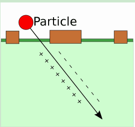
Figure 2: Charged particle striking an integrated circuit and creating electron-hole pairs along its path
When the charged particle hits as shown in figure 3, sequential elements such as shift registers can be disrupted by SEU causing a flipped bit (shown in red) and combinational elements such as AND/OR gates can be affected by a SET which can in turn upset another sequential element further ahead.
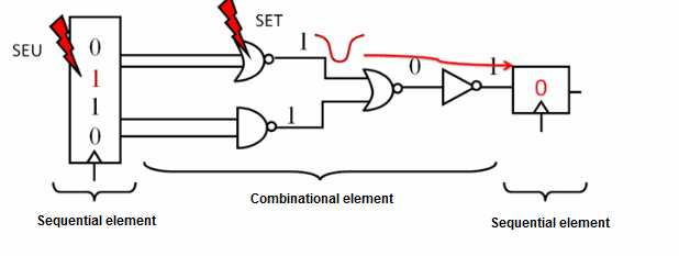
Figure 3: Effect of SEU and SET on sequential and combinational elements in an integrated circuit [Reference 2]
When it comes to providing protection against these charged particles, the integrated circuits can be hard coated or additional substrates such as Silicon on Sapphire (SOS) or Silicon On Insulator (SOI) can be implemented. However, since some nodes in the circuit are more sensitive than others, testing needs to be done prior to the launch of the space instrument to find out exactly where the sensitive nodes are or to verify if the implemented radiation hardening has been strong enough to protect the integrated circuit against the striking radiation. Radiation testing can be either done in a particle accelerator such as a synchrotron or a cyclotron where charged particles are accelerated to simulate the energy of the solar/cosmic particles or it can be done by using ultrashort, pico-joule/nano-joule energy pulsed lasers. The particle accelerator method is more realistic of the actual situation but suffers from several drawbacks including high cost and possibility of inflicting permanent damage to the circuit. The optical method is easier to set up and is less expensive but has several drawbacks. These drawbacks include inability of the optical radiation to penetrate metal and inability to measure the SEE threshold [Reference 3]. Figure 4, shows the optical beam penetrating the non-metal part of an integrated circuit and generating electron-hole pairs along the way.
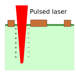
Figure 4: The penetration of pulsed laser into the integrated circuit and generation of electron-hole pairs initiating the Single Event effect (SEE)
For optical testing, a near IR laser of a few kHz repetition rate, pico-joule/nano-joule pulse energy and hundreds of femto-second to one pico-second pulse width is normally used. Utilizing a sensitive microscope, sensitive CCD and InGaAs camera and a very sensitive positional stage, it is possible to determine where the sensitive spots are. Some advantages and drawbacks of optical method were briefly mentioned earlier but some others are mentioned in detail as follows:
● The optical method is restricted by the diffraction limit as far as the focused size of the beam is concerned. For a 1064 nm near IR beam, the diffraction limit is about 1 micron and hence needs to be taken into account.
● Lasers can focus on the device, specifically on the IC chip with sub-micron resolution.
● The optical method is easy to set up anywhere in a lab as opposed to the radiation method which requires an expensive trip to a specific accelerator facility which could be far away.
● The optical technique is perfect for Commercial Off The Shelf (COTS) sorting or pre-screening.
Although the optical technique was compared to radiation technique, it is necessary to emphasize that it is not meant to replace it. Instead, the optical method is meant to be complementary to the radiation method. As mentioned earlier, the optical method can not measure the absolute upset threshold but the laser upset threshold can be compared with the ion beam upset threshold. It is assumed that the relative differences remain the same throughout the measurements and hence all subsequent measurements can be done with the laser [Reference 4]. Calibration of the optical method against the radiation method and the correlation of the two methods will be addressed in a future tech note.
Another factor that needs to be addressed in the optical testing is the possibility of Two Photon Absorption (TPA) as compared to the Single Photon Absorption (SPA) . If the energy of the striking radiation is greater than the band gap of silicon (1.1 eV) then SPA will occur. However, if the energy of the photons is slightly more than half the bandgap (~0.55 eV), then it is possible for two photons to get absorbed and trigger the SEE. The wavelength corresponding to the bandgap is silicon is 1127 nm and hence for two photon absorption, the wavelength of the laser needs to be larger than this wavelength. TPA is a non-linear process and the probability of its occurrence is much smaller than the SPA. However it has the advantage of unlimited penetration depth and well deposited energy in the focal zone due to non-linear absorption. Figure 5 shows the process of TPA and its comparison to SPA.
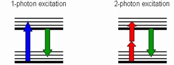
Figure 5: Comparison of SPA and TPA
Allied Scientific Pro has designed a SEE Testing System which uses a NIR laser along with sensitive CCD, SWIR cameras. In addition there is a very sensitive positioning stage and microscope objective which allows the beam to move around the integrated circuit by submicron distances. Figure 6 shows this test system.
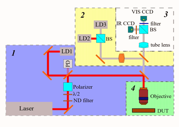
Figure 6: Asp’s SEE Testing System
The system uses Kohler illumination for high contrast shadow free imaging and imaging system with greater than 1.5 megapixels for front side and back side illumination.
References
1- Jeffry Wyss, neutrons for radiation hardness studies, neutron induced single event effects, November, 2009.
2- Fernanda Lima Kastensmidt, SEE mitigation for digital circuit design applicable to ASIC and FPGAs, online presentation.
3- Feng Liang and Steeve Lavoie, 2 Photons; Workstation for Laser Testing of Single Events Effects (SEE) on Radiation Hardened Semiconductor Devices
4- Stephen Buchner, laser simulation of Single Event Effects: A state of the art review, 1995.