Comprendre l'effet d'événement unique (SEE)
Space-borne instruments carry many electronic devices, including microprocessors, digital registers, etc. If a charged particle from space strikes a sensitive node of an electronic circuit, it may cause a disruption or permanent damage. This article intends to explain this issue. Our sun emits a large number of charged and uncharged particles, including protons, heavy ions, and neutrons. Aside from that, there is a constant stream of charged particles from cosmic rays that bombard the Earth. Many of these charged particles get trapped in the Earth’s magnetic field and continuously circle the planet. The Earth’s Van Allen Belt, which traps these charged particles, is shown in Figure 1
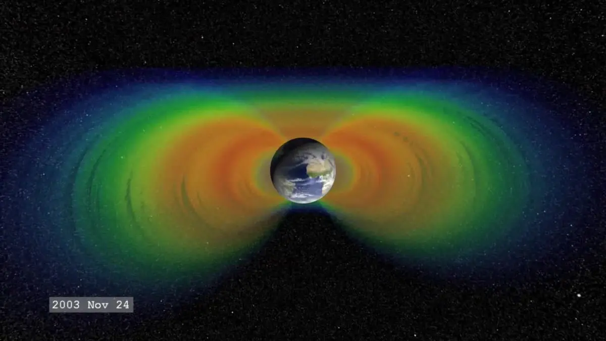
Figure 1 : Ceinture de Van Allen de la Terre (image Wikipédia)
As depicted in the figure, the Earth’s magnetic field is slightly offset from the planet’s axis, and the Van Allen belt consists of an inner belt and an outer belt. In addition, neutrons reaching Earth's surface could collide with an atom and produce a destructive secondary charged particle [Reference 1]. If necessary precautions, such as shielding, are not taken for space instruments, a charged particle striking a sensitive node of the circuit could inflict temporary or permanent damage. These harmful effects on electronic circuits can be classified under a phenomenon called “Single Effect Event (SEE) which can be further divided into sub-categories as follows:
● Trouble d'événement unique (SEU) : un effet transitoire, affectant principalement les souvenirs
● Événement transitoire unique (SET) : une impulsion temporaire traverse le circuit. On ne peut rien y faire.
● Single Event Latchup (SEL) : peut détruire le composant, affectant principalement le CMOS
● Rupture de porte à événement unique (SEGR) : potentiellement destructrice, affectant la structure submicronique
● Single Effect Breakdown (SEB) : A un impact destructeur, affectant principalement les MOSFET de puissance
Certains de ces effets sont uniquement perturbateurs, comme SEU et SET, et d'autres peuvent détruire définitivement un circuit comme SEL, SEGR et SEB.
Circuit quality control testing is required prior to the launch of space instruments to identify sensitive nodes and protect against charged-particle strikes.
La figure 2 montre une particule chargée frappant un circuit électronique et créant des paires électron-trou le long de son chemin.
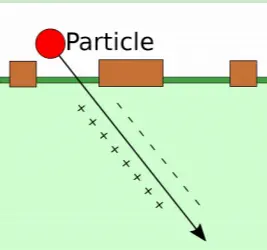
Figure 2 : Particule chargée frappant un circuit intégré et créant des paires électron-trou le long de son trajet
Lorsque la particule chargée frappe comme indiqué dans la figure 3, les éléments séquentiels tels que les registres à décalage peuvent être perturbés par SEU, provoquant un bit inversé (indiqué en rouge) et les éléments combinatoires tels que les portes ET/OU peuvent être affectés par un SET qui peut à son tour perturber un autre élément séquentiel plus loin.
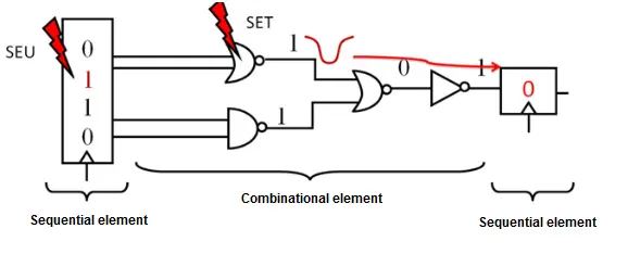
Figure 3 : Effet de SEU et SET sur les éléments séquentiels et combinatoires d'un circuit intégré [Référence 2]
To protect against these charged particles, integrated circuits can be hard-coated, or additional substrates such as Silicon on Sapphire (SOS) or Silicon On Insulator (SOI) can be useTo protect against these charged particles, integrated circuits can be hard-coated, or additional substrates such as Silicon on Sapphire (SOS) or Silicon On Insulator (SOI) can be used. However, since some nodes in the circuit are more sensitive than others, testing needs to be done before launch of the space instrument to identify which nodes are sensitive, or to verify that the implemented radiation-hardening has been sufficient to protect the integrated circuit against intense radiation. Radiation testing can be performed either in a particle accelerator, such as a synchrotron or a cyclotron, where charged particles are accelerated to simulate the energy of solar or cosmic particles, or using ultrashort, pico- or nano-joule energy pulsed lasers. The particle accelerator method is more realistic of the actual situation, but suffers from several drawbacks, including high cost and the possibility of inflicting permanent damage to the circuit. The optical method is easier to set up and is less expensive, but it has several drawbacks. These drawbacks include the inability of optical radiation to penetrate metal and to measure the SEE threshold [Reference 3]. Figure 4 shows the optical beam penetrating the non-metal part of an integrated circuit and generating electron-hole pairs along the way.
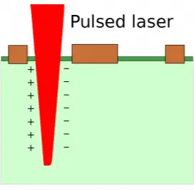
Figure 4 : Pénétration du laser pulsé dans le circuit intégré et génération de paires électron-trou déclenchant l'effet d'événement unique (SEE)
For optical testing, a near-IR laser with a few-kHz repetition rate, picojoule/nanojoule pulse energy, and pulse widths of hundreds of femtoseconds to one picosecond is typically used. Using a sensitive microscope, a sensitive CCD and an InGaAs camera, and a very sensitive positional stage, it is possible to determine the locations of the sensitive spots. Some advantages and drawbacks of the optical method were briefly mentioned earlier, but some others are mentioned in detail as follows:
● The optical method is restricted by the diffraction limit as far as the focused size of the beam is concerned. For a 1064 nm near-IR beam, the diffraction limit is about 1 micron and must be taken into account.
● Les lasers peuvent se concentrer sur l'appareil, en particulier sur la puce IC avec une résolution submicronique.
● La méthode optique est facile à mettre en place n'importe où dans un laboratoire, contrairement à la méthode de rayonnement qui nécessite un déplacement coûteux vers un accélérateur spécifique qui peut être éloigné.
● La technique optique est parfaite pour le tri ou le pré-tri des produits commerciaux sur étagère (COTS).
Although the optical technique was compared to the radiation technique, it is necessary to emphasize that it is not meant to replace it. Instead, the optical method is meant to complement the radiation method. As mentioned earlier, the optical method cannot measure the absolute upset threshold, but the laser upset threshold can be compared with the ion-beam upset threshold. It is assumed that the relative differences remain constant throughout the measurements, and hence all subsequent measurements can be performed with the laser [Reference 4]. Calibration of the optical method against the radiation method, along with the correlation between the two methods, will be addressed in a future tech note.
Another factor that needs to be addressed in the optical testing is the possibility of Two-Photon Absorption (TPA) rather than Single-Photon Absorption (SPA). If the energy of the striking radiation is greater than the band gap of silicon (1.1 eV), then SPA will occur. However, if the photon energy is slightly greater than half the bandgap (~0.55 eV), it is possible for two photons to be absorbed and trigger the SEE. The wavelength corresponding to the bandgap of silicon is 1127 nm, and hence, for two-photon absorption, the wavelength of the laser needs to be larger than this wavelength. TPA is a nonlinear process, and the probability of its occurrence is much lower than that of SPA. However, it has the advantage of unlimited penetration depth and well-deposited energy in the focal zone due to non-linear absorption. Figure 5 shows the TPA process and its comparison with SPA.
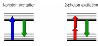
Figure 5 : Comparaison de SPA et TPA
Allied Scientific Pro a conçu un System de test SEE that uses an NIR laser and sensitive SWIR cameras. In addition, there is a very sensitive positioning stage and a microscope objective that allows the beam to move around the integrated circuit by submicron distances. Figure 6 shows this test system.
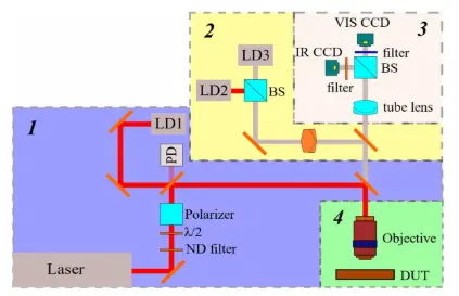
Figure 6 : System de test SEE
Le système utilise l'éclairage Kohler pour une imagerie sans ombre à contraste élevé et un système d'imagerie avec plus de 1,5 mégapixels pour l'éclairage avant et arrière.
Références
1- Jeffry Wyss, neutrons pour les études de dureté des radiations, effets d'événements uniques induits par les neutrons, novembre 2009.
2- Fernanda Lima Kastensmidt, Atténuation SEE pour la conception de circuits numériques applicable aux ASIC et aux FPGA, présentation en ligne.
3- Feng Liang et Steeve Lavoie, 2 Photons ; Station de travail pour les tests laser des effets d'événements uniques (SEE) sur les dispositifs semi-conducteurs durcis aux radiations
4- Stephen Buchner, Simulation laser des effets d'événement unique : un état de l'art, 1995.