Utilisation complémentaire de l'absorption à deux photons (TPA) et des tests SEE des particules
SEE testing of microelectronic devices is complex, and multiple methods may be needed to optimize measurements and obtain accurate error rates. The particle SEE testing method and the laser pulse testing method are the two prominent methods of SEE testing, but neither is perfect on its own. Here are some of the drawbacks of each method:
Méthode des particules :
- The broad-beam particle method will stimulate multiple modes simultaneously, and cross-contamination between them is a problem.
- Il n'y a aucune information spatiale ni temporelle sur l'origine de l'erreur
- For devices with a flipped chip package, the ion beam cannot penetrate the thick dielectric layer to reach the device's sensitive volume.
- The long read-out time will not allow one to determine when the error occurred or what state the memory was in at that time.
Méthode d'impulsion laser :
- L'impulsion optique ne traverse pas le métal. Certains dispositifs microélectroniques sont recouverts de pièces métalliques, ce qui peut poser problème.
- For two-photon absorption (TPA), as described in an earlier technote, variations in device uniformity or laser irradiance can significantly alter the deposited charge due to the square dependence on laser pulse intensity.
- Bien que les tests par impulsion laser démontrent où se trouvent les nœuds sensibles, ils ne fournissent pas une mesure précise des taux d’erreur.
Pour les raisons ci-dessus, il est recommandé d'effectuer des tests par impulsions laser en tandem avec des tests de particules pour un test SEE complémentaire, afin d'identifier les nœuds sensibles, les modes d'erreur possibles et d'obtenir des taux d'erreur précis.
To further analyze the properties of these two complementary testing techniques, SEE testing using a TPA method followed by heavy-ion testing is considered for an SDRAM device [Reference 1]. TPA was chosen for testing this device because the top part was covered in metal. The TPA laser beam could penetrate the device through the backside of the device, which had flip-chip packaging, and illuminate the memory cells. Figure 1 shows the schematic of the TPA testing. The microscope objective focused the beam to a diameter of about 1 micron and passed through the transparent, protective dielectric, with no charge generation in the protective dielectric, since the laser wavelength was longer than the maximum possible wavelength for an electron to traverse the silicon bandgap (1.26 microns).

Figure 1 : Test TPA de la SDRAM
The laser beam produces charge carriers only at its focus when the beam intensity is at its maximum. The micron-sized beam interrogates sensitive nodes of the circuit and eliminates the possibility of cross-contamination of modes that occurs during particle testing. In Figure 2, the microscope objective that focuses the beam onto the part of the circuit with flip-chip packaging is shown.

Figure 2 : L'objectif du microscope focalise le faisceau laser sur le circuit SDRAM
En raison de la dépendance de la section efficace du TPA au carré de l'irradiance, toute hétérogénéité à l'arrière du dispositif testé (DUT) et toute variation de l'irradiance laser modifient considérablement la charge délivrée au volume sensible, ce qui complique considérablement l'évaluation du transfert d'énergie linéaire (TEL) équivalent du faisceau laser. C'est pourquoi les tests particulaires sont indispensables pour obtenir des courbes section efficace/TEL afin de calculer les taux d'erreur. La figure 3 illustre la courbe section efficace/énergie d'impulsion, ainsi que la courbe section efficace équivalente/LET.
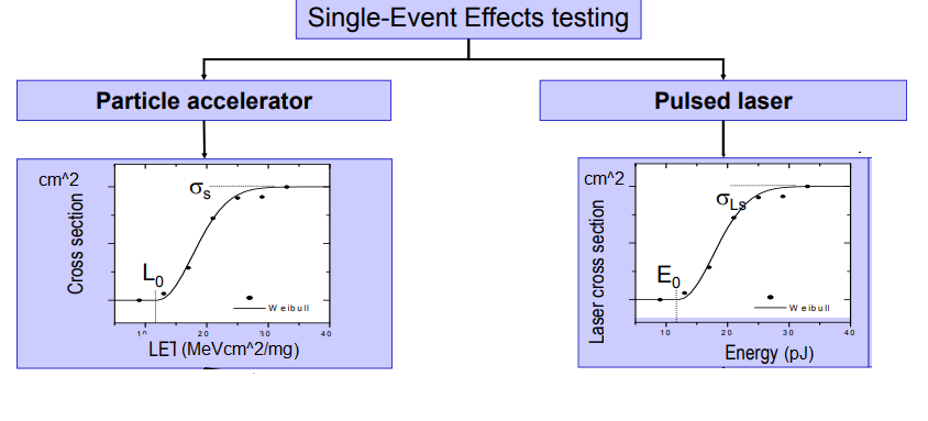
Figure 3 : Comparaison de la section efficace du laser pulsé et de la méthode des particules par rapport aux courbes LET
Dans la figure ci-dessus, σLS, E0. σs et L0 représentent respectivement la section efficace de saturation du laser, l'énergie de seuil SEE du laser, la section efficace de saturation des particules et l'énergie de seuil SEE des particules.
For the SDRAM test, the Device Under Test (DUT) was placed exactly underneath the camera system and the laser beam. Both the IR beam from the illuminator and the laser beam were focused on the sensitive volume. As the translation stage was driven by the laser beam, the device under test was scanned, and the DUT image was observed by the IR camera. A strip along the center part of the SDRAM contained most of the control logic, and its features were resolvable under the microscope as shown in Figure 4A strip along the center part of the SDRAM contained most of the control logic, and its features were resolvable under the microscope as shown in Figure 4.

Figure 4 : La structure en peigne résolue au centre de la SDRAM, observée sur l'image, contenait la majeure partie de la logique de contrôle et était à l'origine de la plupart des erreurs logiques.
Cependant, la matrice de mémoire était située de chaque côté de cette bande au centre de la SDRAM et la résolution du microscope (près de 1 micron) n'était pas suffisamment élevée pour résoudre ses caractéristiques comme illustré dans la figure 5.

Figure 5 : La résolution du microscope n’était pas suffisamment élevée pour distinguer les cellules mémoire individuelles
Les types d’erreurs qui ont été observés lors de ces tests étaient
- SEU (Single Effect Upset), où l'état d'un bit a été inversé
- Minor logic errors, causing 20 upsets
- Erreurs de blocage, provoquant jusqu'à 20-4096 perturbations
- SEFI (Single Effect Functional Interrupt), qui nécessitait un cycle d'alimentation pour la récupération
The TPA testing influenced the heavy ion testing. The main goals of heavy ion testing were to identify SEFI vulnerability, compare the error modes induced in laser and heavy ion testing, and determine cross-section vs. LET curves for different error modes, such as SEU, SEL, and SEFI. One predetermined strategy for the heavy-ion testing was to mask parts of the logic circuit to separate logic circuit errors from memory cell errors. However, the laser testing showed that the control logic is also scattered across the memory array, and therefore, this masking strategy will not be effective.
Several heavy ions were used during the heavy ion testing, including Ne, Ar, Kr, and Xe beams, but a SEFI error could only be observed once during a Kr heavy ion test. The LET for this Kr ion beam was about 22 MeV cm²/mg, and its symptoms of this error mode were very similar to those of laser pulse testing. It required a system reboot to clear, and this error mode likely occurred only during a small part of the SDRAM's operation.
In conclusion, TPA laser testing can be a highly effective tool for evaluating a system's SEE response before heavy-ion testing. Inducing and observing the occurrence of different error modes using the laser-pulse testing method elucidates what to expect during heavy-ion testing, and preparation can be made for test methods, hardware, software, and analysis before a trip to a heavy-ion testing facility.
Allied Scientific Pro has designed a pulsed laser-based SEE testing SPA system that can be upgraded to a TPA system. A video of the system can be found at the following link:
https://photos.app.goo.gl /qRxrgvGaDejq416V8
Référence : R.Ladbury et.al, Tests laser TPA et SEE à ions lourds : techniques complémentaires pour l'évaluation d'événements uniques SDRAM, transaction IEEE sur la science nucléaire (TNS), décembre 2009.